基于FPGA的等精度频率计设计调试(带源码)
今天偶然看到一个有关等精度频率计设计的东西。感觉用处挺大,遂做以研究。
其原理为:如图所示:
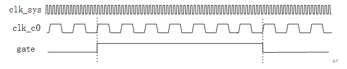
在固定门控时间gate内,通过计数被测时钟的时钟个数cnt1,与基准时钟的时钟个数cnt2,
有 cnt1/(clk_c0) =time_gate 式1
cnt2/(clk_sys) =time_gate 式2
则通过联立两式可计算得被测时钟的频率,如式3
clk_c0=cnt1*clk_sys/cnt2; 式3
下面进行程序设计:系统时钟clk_sys给定为50MHz,为了进行等精度频率计设计,通过pll进行被测时钟clk_c0分频为10MHz,若通过程序设计仿真计算的被测时钟频率为10MHz,则设计成功。
代码如下:
module test ( input clk_sys,//系统时钟50M
            input rst_n,  //系统复位
			output reg[31:0]freq  //输出频率
				 );
//reg
reg gate;
reg gate_clk_c0_1;
reg gate_clk_c0_2;
reg gate_clk_sys_1;
reg gate_clk_sys_2;
reg [10:0]gate_cnt;
reg [10:0]cnt1;
reg [13:0]cnt2;
//wire
wire nege_clk_sys_gate;
wire nege_clk_c0_gate;
wire clk_c0;
 pll_10M  pll_10M(
	.inclk0(clk_sys),
	.clk_c0(clk_c0)
	     );
//门控时钟计数,计数周期1020,门控前后个10个clk_c0时钟周期低电平
always@(posedge clk_c0 or negedge rst_n)begin
  if(!rst_n)
    gate_cnt<=0;
  else if(gate_cnt==1019)
    gate_cnt<=0;
  else
    gate_cnt<=gate_cnt+1'b1;
end
//门控高低电平设计,以被测时钟clk_c0为基准
always@(posedge clk_c0 or negedge rst_n)begin
  if(!rst_n)
    gate<=0;
  else if(gate_cnt<10)
    gate1009)
    gate<=0;
  else
    gate<=1;
end
//在clk_c0域打拍,寻找下降沿
always@(posedge clk_c0 or negedge rst_n)begin
    if(!rst_n)
	   begin
       gate_clk_c0_1<=0;
       gate_clk_c0_2<=0;
	   end
	 else
	   begin
       gate_clk_c0_1<=gate;
       gate_clk_c0_2<=gate_clk_c0_1;
	   end
end
assign nege_clk_c0_gate=gate_clk_c0_2 &(!gate_clk_c0_1);
//在clk_sys域打拍,异步转同步,寻找下降沿
always@(posedge clk_sys or negedge rst_n)begin
    if(!rst_n)
	   begin
       gate_clk_sys_1<=0;
       gate_clk_sys_2<=0;
	   end
	 else
	   begin
       gate_clk_sys_1<=gate;
       gate_clk_sys_2<=gate_clk_sys_1;
	   end
end
assign nege_clk_sys_gate=gate_clk_sys_2 &(!gate_clk_sys_1);
//对被测时钟clk_c0计数cnt1
always@(posedge clk_c0 or negedge rst_n)begin
    if(!rst_n)
	   begin
		   cnt1<=0;
		end
	 else if(gate)
		   cnt1<=cnt1+1'b1;
	 else if(nege_clk_c0_gate)
			cnt1<=0;
end
//对系统基准时钟clk_sys计数cnt2
always@(posedge clk_sys or negedge rst_n)begin
    if(!rst_n)
	   begin
		   cnt2<=0;
		end
	 else if(gate_clk_sys_2)
		   cnt2<=cnt2+1'b1;
	 else if(nege_clk_sys_gate)
		   cnt2<=0;
end
//计算被测信号频率
always@(posedge clk_sys or negedge rst_n)begin
    if(!rst_n)
	   freq<=32’d0;
	 else if(gate_clk_sys_2==0)
	  freq<=(cnt1*50000000)/cnt2;
end
endmodule
在这里插入代码片
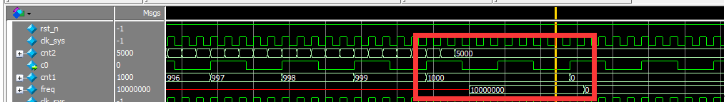
通过Modelsim仿真,给时钟激励和复位信号
仿真结果如图所示:
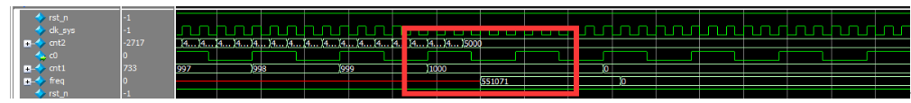
但是发现系统计算的被测时钟频率为551071Hz,和预期分频时钟10MHz不符,仿真显示cnt1=1000,cnt2=5000,系统时钟为50MHz,那么按照式3计算出来的频率应为clk_c0=1,000*50,000,000/5,000=100000Hz。
手工计算的结果并没有用问题,难道是软件计算错误?肯定不会,应该是哪里程序有问题。
捋下思路,查看仿真时序,如图:
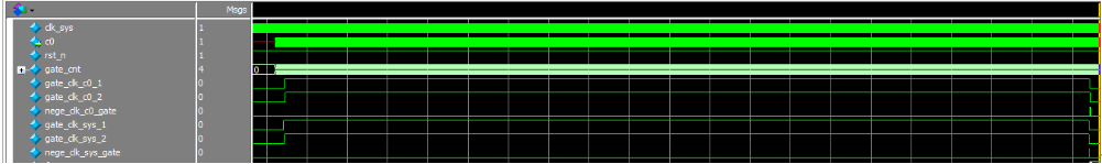
仔细进行对比,发现逻辑时序均无问题。
那么换个角度考虑下551071Hz系统是怎么计算出来的?
使用计算器进行计算,突然发现
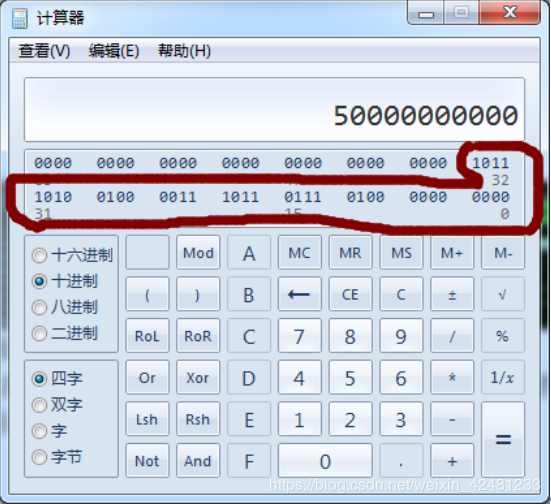
100050000000在计算机中存储位数为35bit,而程序编写时设为32bit
那么改变下频率计算的方式,进行先除后乘,即
Freq<=50,000,000/cnt2cnt1;
编译,仿真,发现
计算结果freq为10,000,000Hz,和预期被测时钟10MHz相等!
由此,看来确实是中间寄存器位宽设计不够。
再做下验证,程序预设位宽为32bit,那么只截取32bit数据
1010 0100 0011 1011 0111 0100 0000 0000
进行计算,发现计算结果为551071.9488,和首次仿真结果551071Hz相同,由此,找到了问题,也解决了问题。
一个公式计算顺序的变化竟会引起海啸!!!
沉思中……
作者:Dr.pp